Skip to content Skip to navigation

Plasma activated direct bonding of silicon and lithium niobate thin films

Project Type: 
E241
Date: 
June 2021
Areas of Interest: 
bonding of pieces, metasurfaces, wave guides
Processing Technique (former Function and Method): 
Researchers and (Mentors): 
Sahil Dagli, Baba Ogunlade (Usha Raghuram), (Swaroop Kommera), (Vijay Narasimhan)
Nano Nugget(s): 

Our E241 students demonstrate their technique for bonding pieces of Si and LiNb with tweezers.

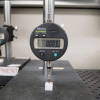
The drop gauge is a simple to use, tabletop vertical displacement measuring device in SNF. It has micron level resolution and can be used to characterize micron to millimeter scale etch rates.

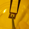
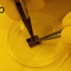
When bonding plasma activated surfaces together, it is important to apply a sufficient amount of force to the chips when pressing them together to properly initiate the bond. Pressing with tweezers is an easy and effective, as well as tricky way to do this. Check out the tips and tricks!